|
ELECTRONIC ASSEMBLY
ELECTRONIC COMPONENTS
PCB
SMD STENCILS
MACHINING


|
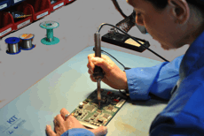
ELECTRONIC ASSEMBLY
Technical Capabilities:
• Machine placement of SMT components down to 0402,
• up to 50mm square, BGA, uBGA, fine pitch QFP
We offer a comprehensive range of services that includes:
• purchases of components and/or PCBs;
• SMD Solder Stencil;
• smt electronic assembly;
• through hole technology (THT);
• visual inspection of PCBs;
• upload a software;
• testing;
• packaging and shipping.
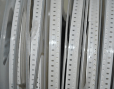
ELECTRONIC COMPONENTS
We offer a variety ways to provide material for the production of:
1. Assembly of electronic componets supplied by the customer.
2. We buy components for your order, and then we use them to your assembly;
Some orders require the use of special components - according to customer specifications - such as EMC screens, mechaning, various transformers, etc...
We offer a performance of such components in the production order.
PCB
We are a provider of high quality printed circuit boards. Thanks to contacts with manufacturers PCBs, we are able to provide any PCB's in any quantities.
The quality of our PCBs is confirmed:
• a written report of qualitative research (including electrical testing);
• Certificate of compliance with the RoHS Directive;
• 24-month warranty against defects in materials.
Our PCBs are made in accordance with a quality standards IPC-A-600. As the format of the data in the format we prefer gerbera RS-274X.
Specifications:
Standard design of printed circuit boards
|
Material
|
FR4/1,6mm
|
|
Layer
|
2L
|
|
Finished Copper Thicknes(OZ)
|
35um (1 OZ)
|
|
Soldermask
|
Green
|
|
Silkscreen
|
White
|
|
Finishing
|
Immersion gold or HAL Lead Free
|
Technological parameters of printed circuit boards
Maximum number of layers
|
22
|
Maximum panel size
|
750 x 600 mm (30'' x 22'')
|
Maximum panel thicknes
|
0,2-4,8mm ±10%(>1.0mm)
|
The minimum thickness of the multilayer board
|
4 layers: 0,38mm (15mils)
6 layers: 0,55mm (22mils)
8 layers: 0,8mm (32mils)
10 layers: 1,00mm (40mils)
|
The minimum diameter of the hole
|
0,15mm (6mils)
|
The minimum Track/Gap
|
0,075mm (3mils)
|
Cu weight
|
outers: 1-6 OZ
innters: 1-4 OZ
|
Gold weight
|
10u'' or 30u''
|
Bending and twisting
|
≤1.0%
|
Test voltage
|
50~380V
|
V-cut
|
30°/45°/60°
|
SMD STENCILS
We offer SMD stencil made in the following technologies:
1. Prototype SMT Stencils – their advantage is the low price, but they are suitable only for plates with large SMT solder and have a limited life
2. Laser Cut SMT Stencils – provide the best possible quality and longest life
Laser stencils are made of laser sheet thickness: : 0.1mm, 0.12mm, 0.13mm, 0,15mm, 0,18mm 0.2mm.
Prototype stencils made of laminate thickness 0,25mm.
The data to perform strencil we prefer gerbera in RS-274X.
MACHINING
Precise milling, drilling, engraving, plotting. We offer you the service of processing of plastic and metal enclosure to order.
In addition, we can placed on these enclosure inscriptions or drawings by screen printing.
The accuracy and aesthetics guaranteed!
We encourage you to submit a request for quotation!
|


